Requirements
Market · product standards · ports · performance criteria
Use schematic and PCB methods from the core reference to organize six design domains into a reviewable, verifiable, and regression-ready engineering system.
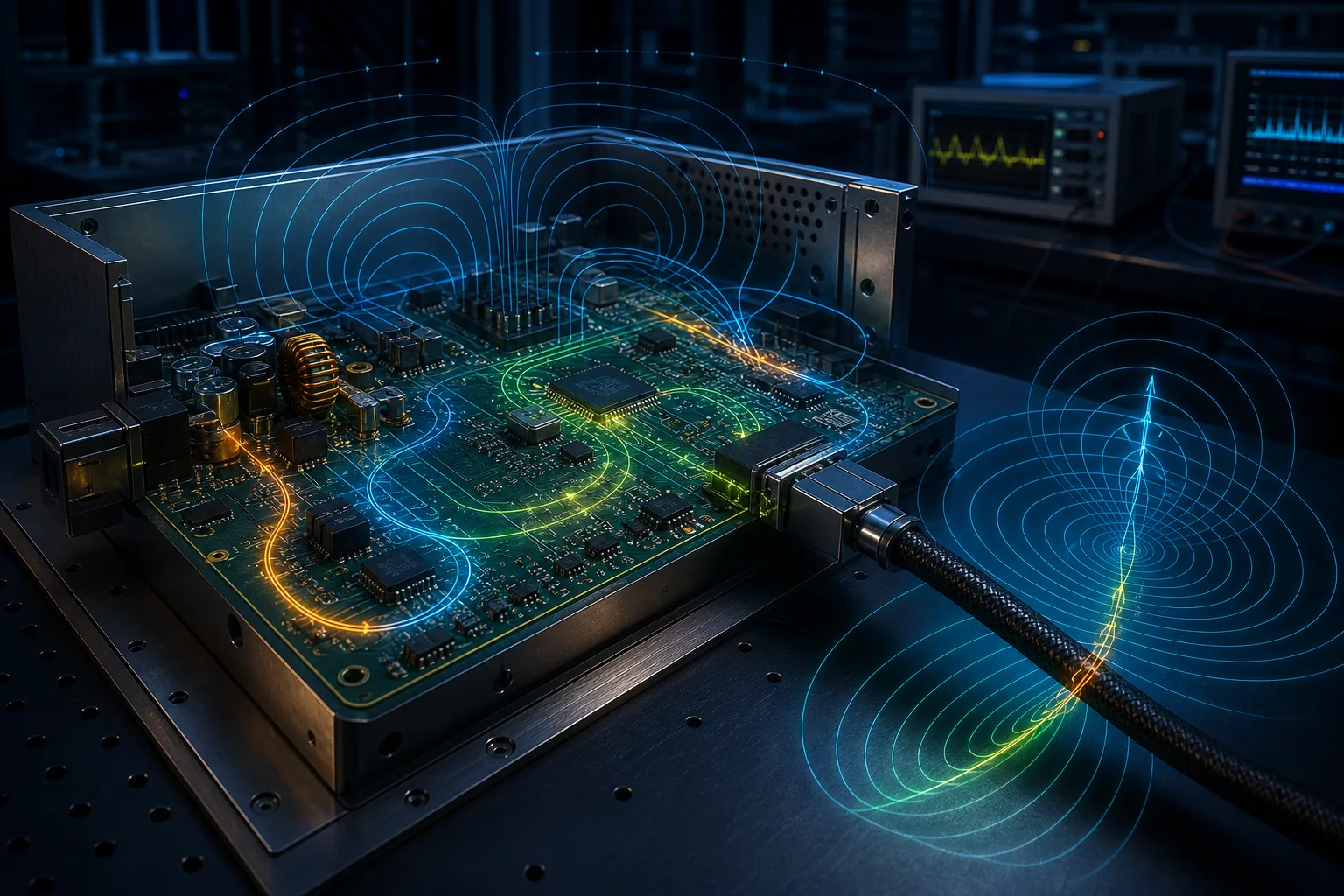 ENERGY / RETURN / COUPLING / PROOF
EMC is not a post-layout check. It begins with requirements and architecture and continues through production changes.
Market · product standards · ports · performance criteria
Noise sources · sensitive domains · chassis and harness topology
Edge control · filtering · isolation · clamping · provisions
Stackup · return paths · hot loops · interfaces · shield termination
Baseline spectrum · near-field map · common-mode current · immunity threshold
Worst-case modes · margin · reports · change regression
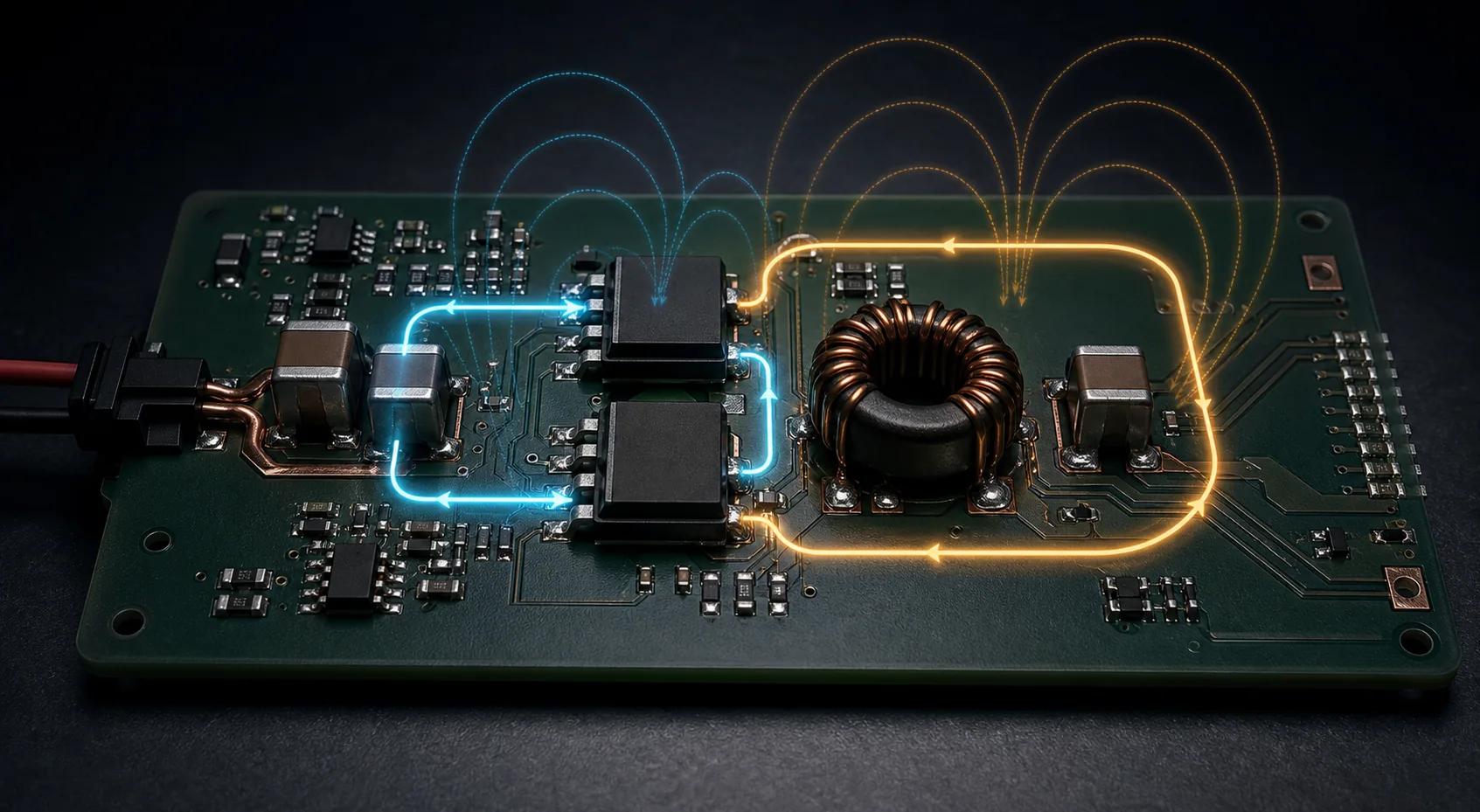 01 / POWER / HOT LOOP
How small is the high-di/dt loop, and how large is the high-dv/dt copper area?
02 / CLOCK / SPECTRUMIs emission bandwidth governed by clock frequency or edge rate?
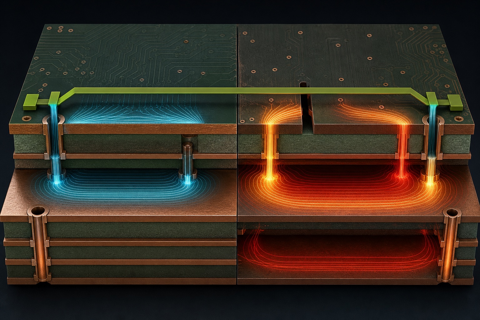 03 / STACKUP / RETURN
Does every critical trace have an adjacent, continuous reference through layer transitions?
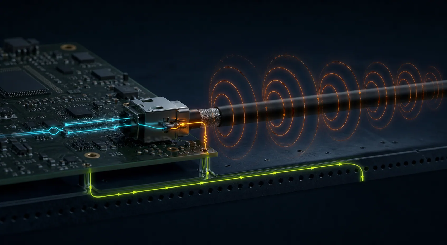 04 / I/O / COMMON MODE
Where can differential imbalance convert into cable common-mode current?
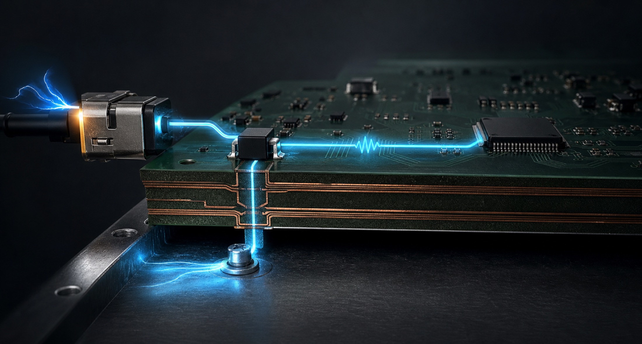 05 / TRANSIENT / DIVERSION
Can pulse current be diverted through a short, wide path before it reaches sensitive circuitry?
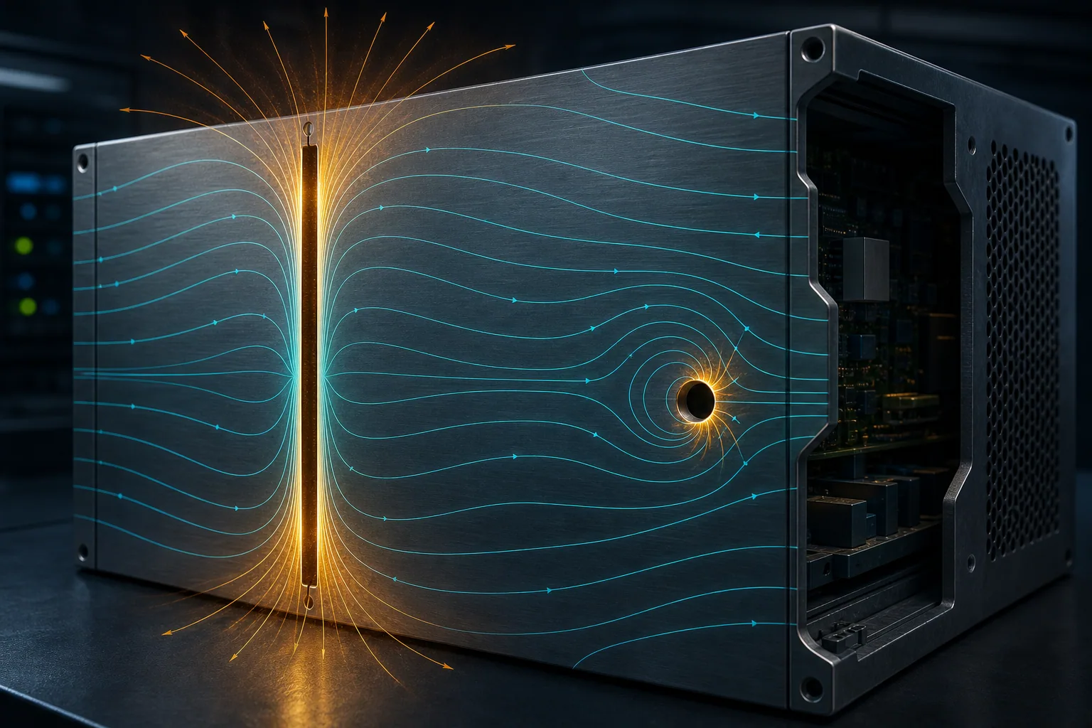 06 / SHIELD / APERTURE
Which seam interrupts surface current, and where does the cable shield terminate?
The edge-spectrum model turns clock, damping, and component-substitution risk into discussable quantities.
Use fedge ≈ 1/(πTr) to estimate the trapezoidal edge-spectrum breakpoint. It is not a hard cutoff; package, drive impedance, ringing, and duty cycle alter the measured spectrum.
Plane splits, layer transitions, and vias are not isolated rules; each changes high-frequency return geometry and impedance.
Example geometry: 50 mm signal length and 0.2 mm reference spacing; the split case uses a 20 mm detour width and 110 mm return path. Real current distribution requires stackup-aware 3D analysis or measurement.
Self-resonance and parasitics determine whether a component behaves as capacitance, inductance, or a new resonance in the target band.
This is why more capacitance does not necessarily improve high-frequency EMI. Component, package, layout, source impedance, and load impedance must be verified together.
Place the TVS in the complete diversion loop to evaluate residual voltage among connector, chassis, and sensitive IC.
The protection device sits at the connector, so current reaches the TVS before the protected trace and the diversion loop avoids sensitive circuitry.