01P01—24
Physical foundations
Explain behaviour through edges, return paths and coupling
- Voltage transients
- Signal return paths
- Common / differential mode
- Reflection and crosstalk
- High-frequency component models
Start with energy and complete current loops, then move into schematics, PCB geometry, interfaces and test cases. Global primary sources add evidence, boundaries and standards status without changing this physical spine.
Each layer answers a different question: why it happens, how to design, how to implement and how to verify.
Explain behaviour through edges, return paths and coupling
Create controlled paths for interference current
Implement return-path continuity in physical geometry
Verify with frequency, paths and single-variable experiments
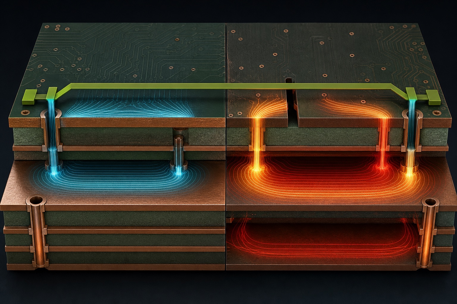 FOUNDATION / RETURN CURRENT
Forward and return paths jointly determine impedance, radiation and immunity. Ground is not a symbol but a frequency-dependent current path; splits, layer transitions, connectors and protection devices belong in the same closed-loop analysis.
Example geometry: 50 mm signal length and 0.2 mm reference spacing; the split case uses a 20 mm detour width and 110 mm return path. Real current distribution requires stackup-aware 3D analysis or measurement.
They look different but share one mechanism: RF impedance pushes current into an unintended path. The interactive models turn static guidance into an operable decision.
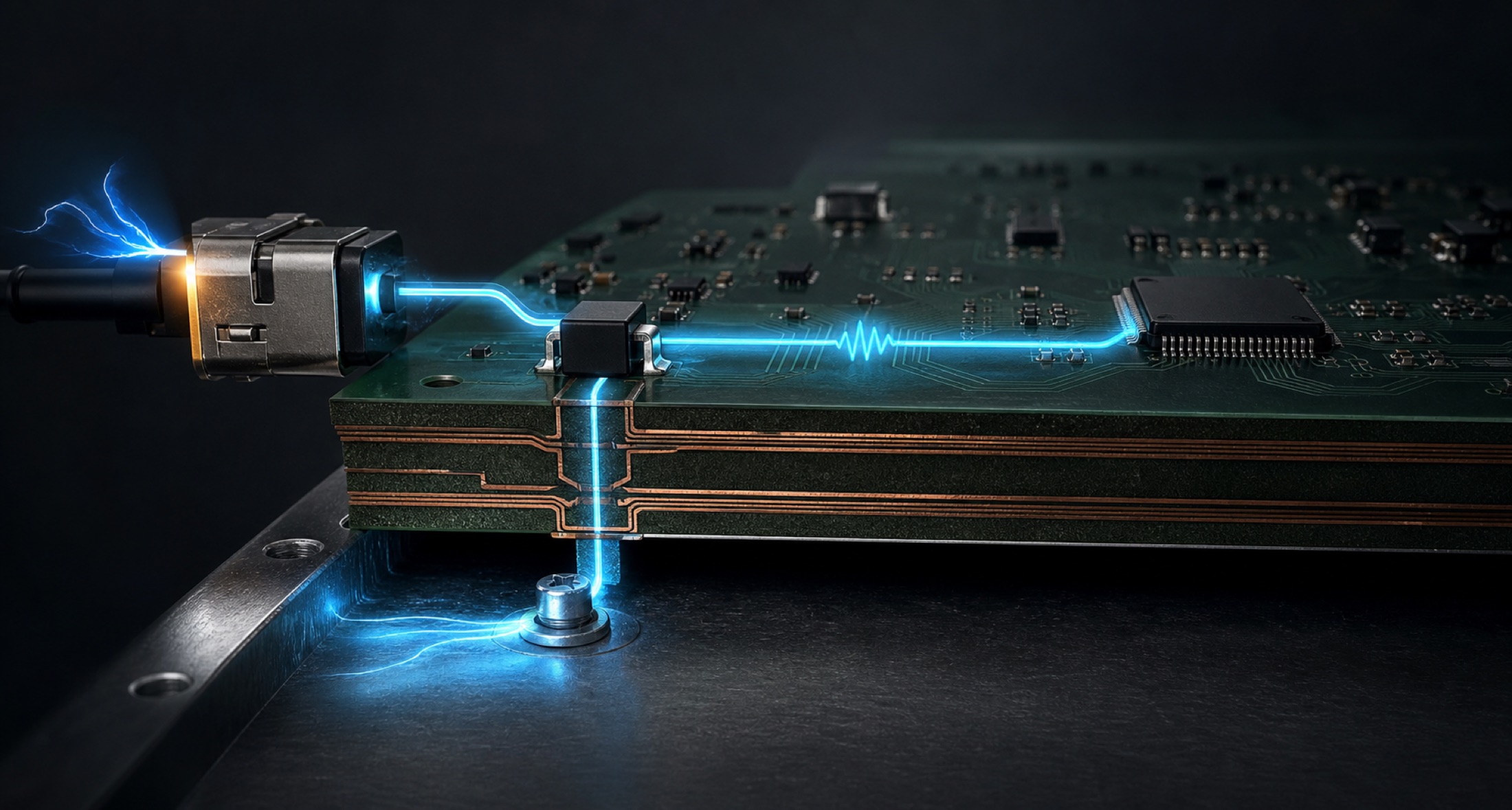
The protection device sits at the connector, so current reaches the TVS before the protected trace and the diversion loop avoids sensitive circuitry.
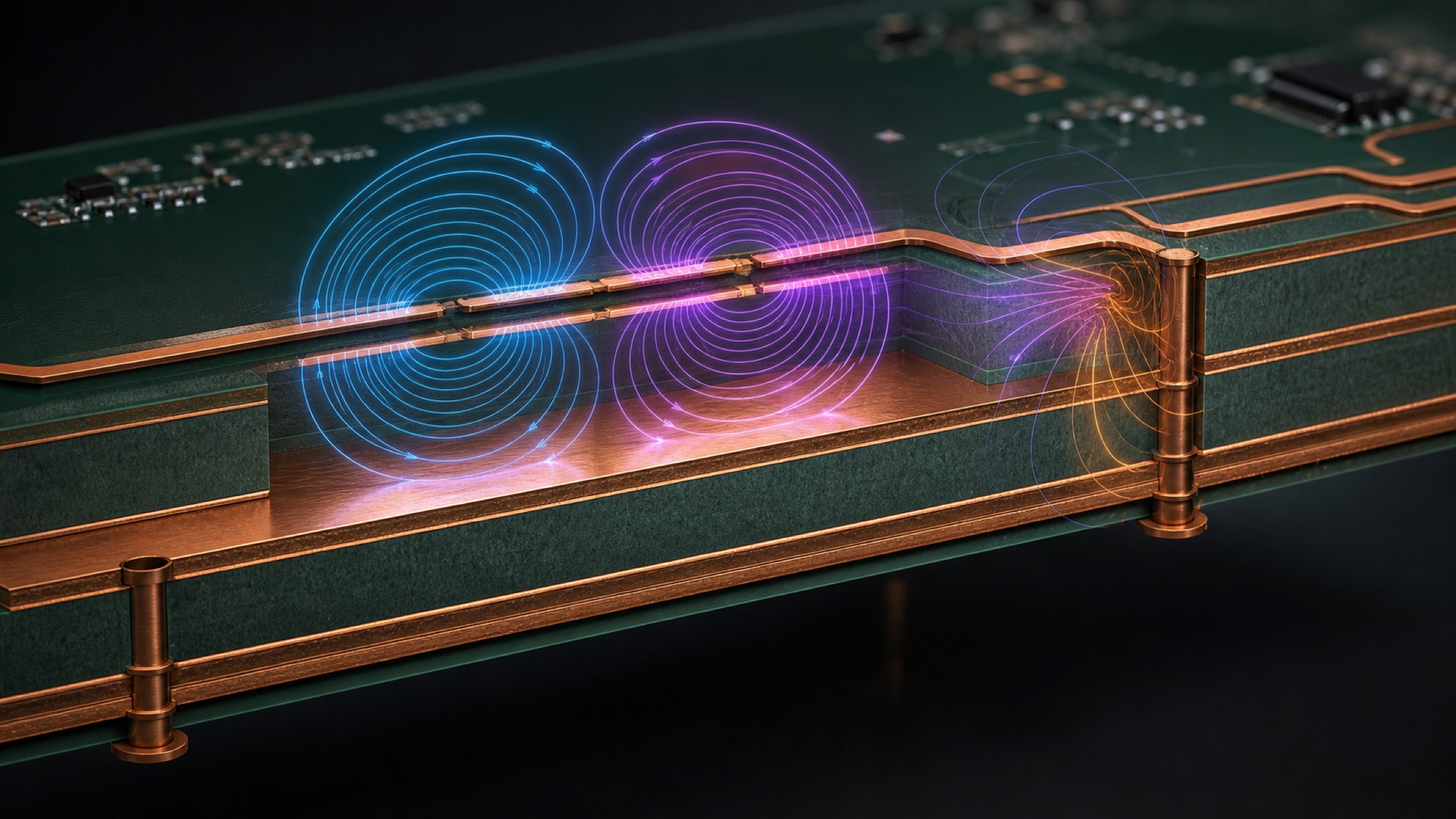 DIFFERENTIAL BALANCE / COMMON-MODE CONVERSION
Pair length, spacing, reference plane and adjacent geometry jointly determine common-mode conversion. A continuous reference remains essential because any asymmetry leaves a common-mode component that must return.
Explore differential and high-speed interface resources ↗Each case connects frequency relationships, physical paths, verification actions and the final redesign, turning experience into reusable engineering evidence.
DiagnosisCLK133 runs parallel to the USB differential pair over a long distance with asymmetric via geometry.
ActionIncrease spacing between the clock route, the differential pair and their vias.
DiagnosisFunction is unchanged, but faster edges in the new lot extend EMI bandwidth.
ActionInclude component substitutions in power, signal-integrity and EMC regression tests.
DiagnosisThe panel LED signal carries internal noise to the RJ45 and external cable.
ActionRestore the reference and bridge return, then slow and filter the source edge.
DiagnosisClock-driver noise enters the interface IC through shared supply impedance and radiates from the cable.
ActionIsolate the clock supply domain and verify supply impedance and common-mode current.
DiagnosisFive optocouplers provide roughly 10 pF of aggregate parasitic capacitance and form a common-mode path.
ActionProvide a controlled common-mode bypass and reduce digital-ground path impedance.
DiagnosisA TVS far from the main path adds branch inductance and raises residual voltage at the sensitive node.
ActionPlace the TVS at the connector with flow-through routing and a short discharge loop.
Each supplementary source closes one defined gap: edition status, test boundary, component parameter or modern high-speed layout.
Continuous reference planes and shortest return paths
TI SCAA082A ↗02HIGH-SPEED I/OHigh-speed interfaces and flow-through ESD layout
TI SPRAAR7J ↗03SYSTEM ESDTLP data, device parameters and system-level protection
Nexperia ↗04GROUND / CABLEReturn-current spreading and cable common-mode noise
Murata ↗